

Atari ST OPL3 cartridge prototype pcb’s arrived
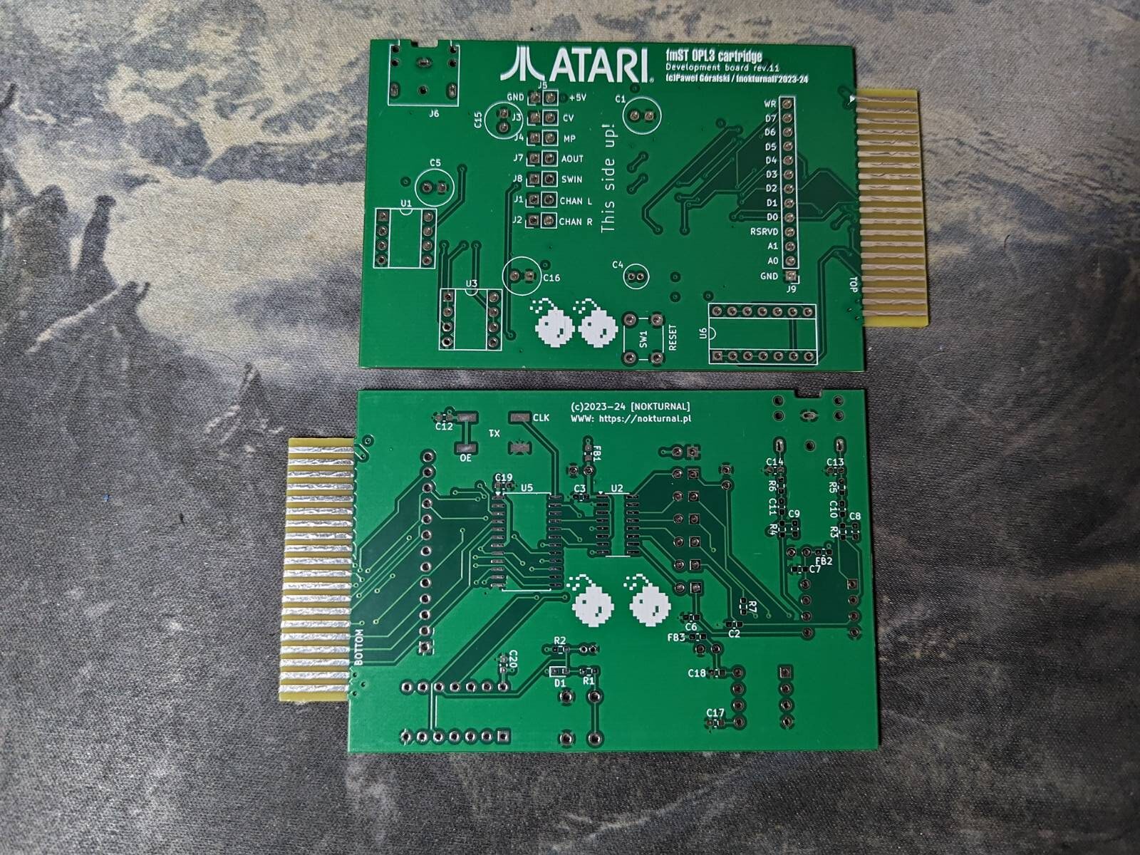
Few days ago I’ve received test batch (5pcs) of Atari ST OPL3 cartridge pcb’s. It was suprisingly fast process, it took exactly week.
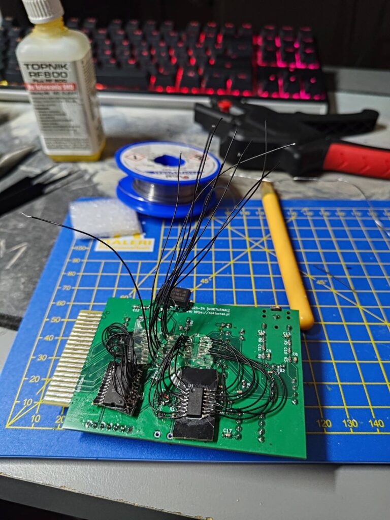
Two major issues came out after I’ve reviewed it. Firstly I’ve inserted wrong footprints for OPL3 / DAC, instead my custom / tested ones I’ve used default KiCad footprints, which were smaller, this gave me a lot of headache during assembly and significatly increased soldering time.
Additionally my custom footprint for clock generator SG-615P also turned out to be too small. Other than that, test cart pcb was 1mm too wide on both sides, so it doesn’t fit in standard, short ST case. For prototype it doesn’t matter (it can be readjusted with Dremel tool), but it’s important thing to note for final version and certainly I need to verify cartridge size with Mega ST case. STe / Mega STe / TT should be fine. Pcb width reduction should also accomodate cartridge case thickness.
So, this is lesson for future to make 1:1 print outs of pcb, before ordering. I’ve done it last time, but not this time and here’s result.
Other than that I came into conclusion that I could add capacitor polarity markings, numbering of cartridge pins, SMD diode could be THT (I’ve got issues with sourcing SMD ones), C4 capacitor could be little bigger (also all capacitor polarity could be arranged in uniform manner e.g like minus on left side, plus on the right side of pcb) and reset switch button could be smaller. I also thought about adding a pin with generated clock (it’s hard to access from the bottom) and place to plug external DC source (for tests without plugging pcb into computer). But that’s rather development, assembly QoL things.
I had to make 30 degree cartridge edge to not ruin ST cartridge port (,which nowadays is not easy to get or replace), maybe for final version I will decide to do it on manufacturer side along with SMD parts soldering (depending on costs).
Other than that everything looks fine for now.
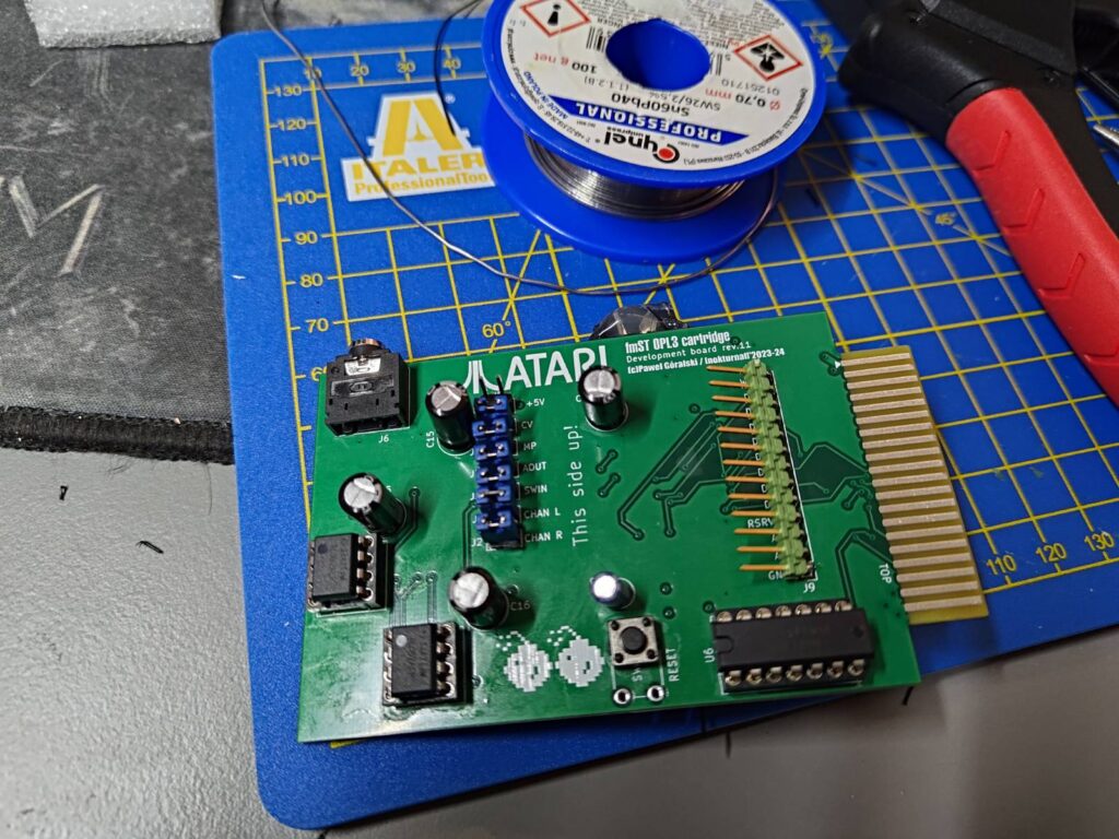
Here’s assembled prototype. Top looks nice, bottom not so, because I had to solder pads with kynar to SOP / SMT chips, which were soldered to pcb adapter boards I’ve made at the beginning of the project to use OPL3 / DAC with THT elements and bradboards, but had to repurpose and cut them a little.
This is how soldering finish line looked like. And I thought that SMD 603 elements will be my biggest issue here :) :
Assembled prototype:
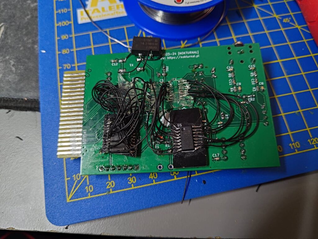
I’ve made some checks with multimeter to make sure if there aren’t any short circuits or other issues like mismatched signals. I’ve caught one short of two OPL3 data lines, which were result of very late soldering session, this wouldn’t occur if footprint’s were ok from the start and of course one capacitor in reset circuit was inserted the other way. Probably I will order another batch of prototype pcb’s with correct footprints.
So next step will be adjusting pcb a little and checking cart on real hardware. If it will not blow up or fry I think it will be major success :)..
If everything will be fine, next stage will be testing adress line settings, clock generation, opl3 operation and DAC output etc..
O wpisie
Aktualnie czytasz “Atari ST OPL3 cartridge prototype pcb’s arrived,” wpis w [nokturnal].
- Opublikowano:
- 24 April 2024 1:44 AM
- Kategoria:
- Atari 16/32 bit, Falcon 030, Hardware, OPL3 (YMF262), ST/STe, TT, Wieści
Brak komentarzy
Skocz to formularza komentarzy | komentarze rss" [?] | trackback uri [?]